Wednesday, April 5, 2023
Perfect imperfections: how AWS is innovating on diamond materials for quantum communication with Element Six
Color centers in diamond are a leading technology platform for quantum communication and networking. In this announcement, we introduce you to key concepts of quantum communication and discuss how diamonds can be used in quantum networking nodes. We are also announcing a new research collaboration with Amazon Web Services (AWS) to explore ways to develop and improve synthetic diamond for quantum networking.
Quantum networks: entanglement distribution over long distances
Quantum networks use the properties of entanglement and superposition to securely distribute quantum information between network end users. These networks consist of two types of nodes - backbone nodes and end user nodes - each of which rely on different types of technology. End user nodes can use traditional telecommunications resources like lasers and detectors to communicate with the backbone nodes. Backbone nodes, on the other hand, will require a new type of infrastructure: a quantum repeater. These repeaters serve a similar function as amplifiers in classical communication networks by correcting for loss and infidelity which occurs as quantum information propagates over long distances, but are able to do so without disrupting the quantum state of light that passes through the network. This makes it possible to correct the unavoidable scattering of individual particles of light, known as photons, as they pass through even the best telecommunications fiber. As such, these repeaters make possible the spread of quantum information over distances that would otherwise be impossible due to photon loss.
Quantum repeaters will act as the backbone for a future quantum internet which will enable secure and private communication - making them a central focus for research at the AWS Center for Quantum Networking.
The core element of a quantum repeater is a memory qubit which interfaces with light. This qubit catches the information encoded on light, stores it, and, together with other nearby qubits, performs error correction to eliminate any errors which may have occurred during communication. To be viable, these memory qubits need to have reliable interactions with light in the visible or telecom domain (ruling out many of the leading qubit candidates from quantum computation, such as superconducting qubits) and preferably be feasible to mass-produce. These requirements make defect qubits, like color centers in diamond, leading candidates as quantum repeater memories.
Defective but not broken
Defects in solids are a wide class of qubits which consist of one or more atoms forming a defect inside an otherwise uniform, crystalline material. Depending on the type of atom and material used, the qubit is defined from the electronic or magnetic states of the defect atom(s). Defect qubits are found in many materials naturally, and can often be introduced artificially through the targeted implantation of a host material with the defect atom of choice. Despite so many materials being capable of hosting defect qubits, finding a material-defect pair that has any specific combination of properties is a challenging task.
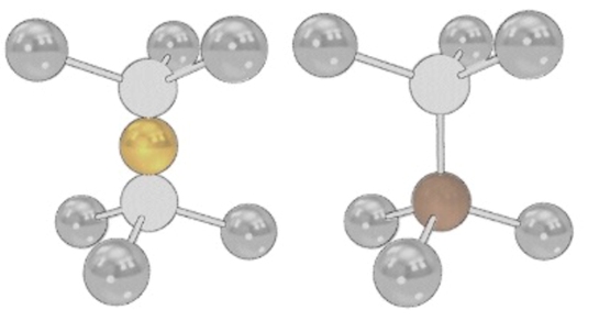
These diagrams of the NV (left) and SiV (right) show their atomic configuration inside the diamond lattice. In each case carbon atoms (silver) are displaced by vacancies (white with black outline) and defect atoms (Nitrogen in brown, Silicon in gold). Source: AWS Center for Quantum Networking.
Diamond is one of nature’s most remarkable materials. Diamond, formed from a lattice of carbon atoms, is the hardest natural material in the world, has the widest optical transmission, and is the best naturally occurring thermal conductor. It is stable in environments ranging from the deepest, coldest vacuum up to immensely high pressures and temperatures - and can even safely be integrated into the living bodies. Natural diamond forms deep inside the earth as a result of tectonic pressures 100s of kilometers below the earth’s surface. These diamonds, as a consequence of their growth environment, are varied and unique. Despite being more pure than other natural crystals, contain many different impurities incorporated from the environment during the long, slow growth process.
These impurities are what give diamonds their widely ranging colors - ranging from deep blue to bright pink. In certain cases, however, defects in diamond do more than make them unique and beautiful: they can also act as exceptional qubits for quantum networking applications.
Diamond hosts many different defects, but two classes of diamond defect qubits have emerged as leading candidates for communications applications: the Nitrogen-Vacancy Center (NV) and the Silicon-Vacancy Center (SiV). Both the NV and SiV are formed by removing two adjacent Carbon atoms from a diamond crystal lattice, and replacing them with a single Nitrogen or Silicon atom, respectively.
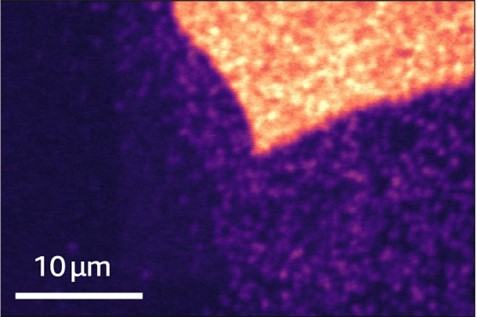
Atomic defects embedded in diamond can change the way it interacts with light. Here, an Element Six high purity PECVD-grown diamond is implanted with SiV (top right) and NV (bottom right), and annealed. When irradiated with green light regions of pure diamond (left) then emit no light, where regions with defects produce different intensities of red light, producing the preceding image. Source: AWS Center for Quantum Networking.
Remembering light
Quantum repeaters operate by transferring information encoded on photons onto a stationary memory qubit where the information can be stored and corrected. Defect qubits, such as color centers, are good candidates for this operation because they naturally have an effective interface with light (the source of their color) and because a subset have access to a long lived “spin” memory. This spin can be thought of as a tiny magnet contained inside every electron, proton, and neutron within the material. This spin memory can be accessed by placing the qubit in a magnetic field such that the spins orient along the direction of the field. The memory is then defined by whether the spin is pointing along or opposite the magnetic field, which corresponds to a 1 or 0 bit respectively. When light bounces off a color center it can flip this spin qubit, making possible the transfer of information between light and the spin memory in what is known as a spin-photon interface. Color centers with this property - such as the NV and SiV - are useful candidates for quantum repeaters.
The NV and SiV are different from other color centers by being hosted in diamond, which is compatible with a wide variety of semiconductor processes and is chemically inert and stable under many different environments. This means that these qubits can be positioned inside nanoscale devices engineered for specific applications. NVs, for example, are often placed at the tip of a scanning probe for microscopy, or at the center of a hemispherical lens or pillars used to collect light efficiently. SiVs, which are less sensitive to the environment, can be placed inside even smaller structures. They are commonly used inside waveguides and photonic crystal cavities just 100s of nanometers across.
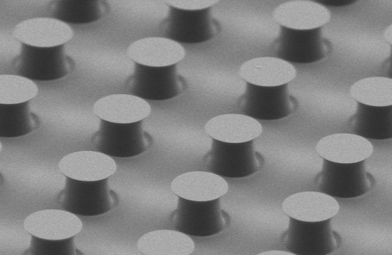
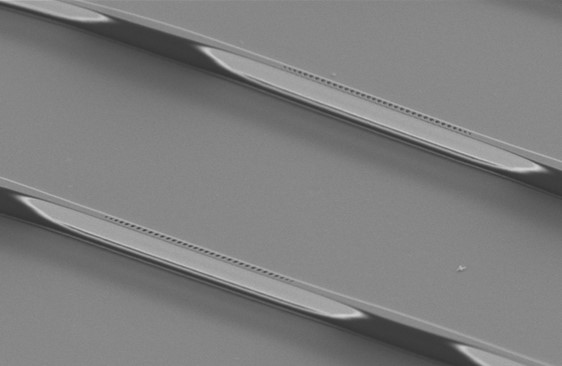
First Image: Diamond pillars used to enhance the collection of light from color centers. Second Image: Photonic crystal devices made from diamond used to ensure deterministic interactions between color centers and light. Source: AWS Center for Quantum Networking.
The SiV is a part of a well-studied class of defects, known as “Group IV” defects, given by their location on the periodic table, which are notable for their low sensitivity to magnetic and electric field fluctuations, which occur at the surfaces of most materials. This reduced sensitivity makes it possible for the SiV to be placed inside smaller structures - which in turn improves the reliability with which they interact with light. A SiV defect also has other properties that make it well suited for quantum networking operations. It has a coherence time of up to 10 milliseconds, and a secondary, nuclear spin memory that can live more than a second. SiVs can be controlled and read out individually with high accuracy, with 99.98% readout fidelity, single qubit gate fidelity better than 99%, and spin photon gate fidelity better than 95%.
Using Element Six’s synthetic diamonds, these features have been combined by a team of Harvard and MIT scientists to enable memory enhanced quantum communication, a benchmark that means that the SiV will enable communication over distances longer than would be possible without repeaters. Engineering and scaling up the technology surrounding the SiV should make widespread deployment of this technology possible— and this engineering starts with the diamond material itself.
Exploring new synthetic diamond solutions for quantum networking
In natural diamond the number of undesired defect atoms reduces the coherence, optical, and spin properties of color centers like the NV and SiV. Fortunately, the advent of synthetic diamond growth has made reducing these undesired imperfections possible. Advances in plasma-enhanced chemical vapor deposition (PECVD) over the last 20 years have enabled the growth of individual plates of diamond with sufficient purity and orderliness for quantum applications. PECVD growth enables the formation of diamonds hundreds or thousands of times purer than the Regent Diamond, the famously pure natural diamond on display in the Louvre. In the best PECVD diamond less than one in a million atoms are impurities - compared to one in a thousand for most natural diamonds.
Continuing to invest in PECVD diamond technology will be critical to enabling its utilization for quantum applications. Improving control over the types of defects created and material incorporated during diamond growth, widening the different morphologies of diamonds which can be mass produced, and reducing the cost of their manufacture will be critical to the advancement of this field.
Announcing a new collaboration between AWS Center for Quantum Networking and Element Six
Diamond’s optical and quantum properties make it uniquely promising for quantum networking and quantum communications applications – but lack of widespread access to different grades and morphologies of diamond has long been a challenge for the field. Element Six and AWS are working together to develop new technologies to make diamond a more flexible and accessible material – helping drive growth and progress for this technology.
Today, AWS is announcing a new research collaboration with Element Six to explore ways to develop and improve synthetic diamond for quantum networking.
When it comes to innovation and technology, materials matter
Synthetic diamond is a leading solution for applications in quantum communication, where the material can be used as a node in the development of quantum networks. Diamond memory nodes help grow networks by facilitating quantum communication over long distances – a challenge requiring quantum memory nodes with efficient optical interfaces and long memory times.
Leveraging decades of experience
The potential of diamond for this field was first recognized by groups more than 10 years ago, including by Element Six, now an AWS Center for Quantum Networking collaborator.
With over 70 years of technical expertise in developing growth technology and application know-how of synthetic diamonds, Element Six has pioneered diamond solutions across many disruptive areas, including oil and gas exploration, water treatment, advanced thermal management for high performance semiconductor devices and optical applications in fusion energy and EUV lithography.
Working with leading academic partners in the U.S. and Europe, Element Six was the first to show synthetic diamond could be produced with properties tailored for quantum applications.
While the field still presents many fundamental and technical questions, this collaboration between AWS and Element Six aims to develop a scalable synthetic diamond solution consistent with efficient photon-spin interaction and control, which could be used to advance the development of quantum technologies, including secure networks, sensors, or computers, in the future.
To learn more about AWS’s quantum efforts and get started, visit the AWS Quantum Technologies Homepage.
About the authors
- Dr Bartholomeus Machielse
Quantum Research Scientist in the AWS Center for Quantum Networking
- Dr Daniel Twitchen
Executive Director, Element Six
Business Development & Technologies Sales
About Element Six
Element Six, part of the De Beers Group, is a world leader in the design, development and production of synthetic diamond and tungsten carbide supermaterials. We operate worldwide with primary manufacturing facilities in Germany, Ireland, South Africa, the UK and US. Since 1946, Element Six leverages the extreme properties of synthetic diamond to open up new possibilities in areas such as quantum optics, acoustics, power transmission, water treatment, thermal management and sensors. Element Six supermaterials solutions are also used in a wide range of applications across multiple industries, including manufacturing in the Automotive and Consumer Electronics industries, cutting and drilling in the Oil & Gas industry, and in components for Mining, Road & Wear applications.
Element Six Media Contacts
- Gabriella Sciarrone
Head of Marketing and Communications
gabriella.sciarrone@e6.com
e6@speedcomms.com
